Here is a general ISP (In-System Programming) pin-out diagram for the BGA 254 / eMMC / eMCP package (commonly used in many smartphones).
Key Signals & Typical Pin Functions
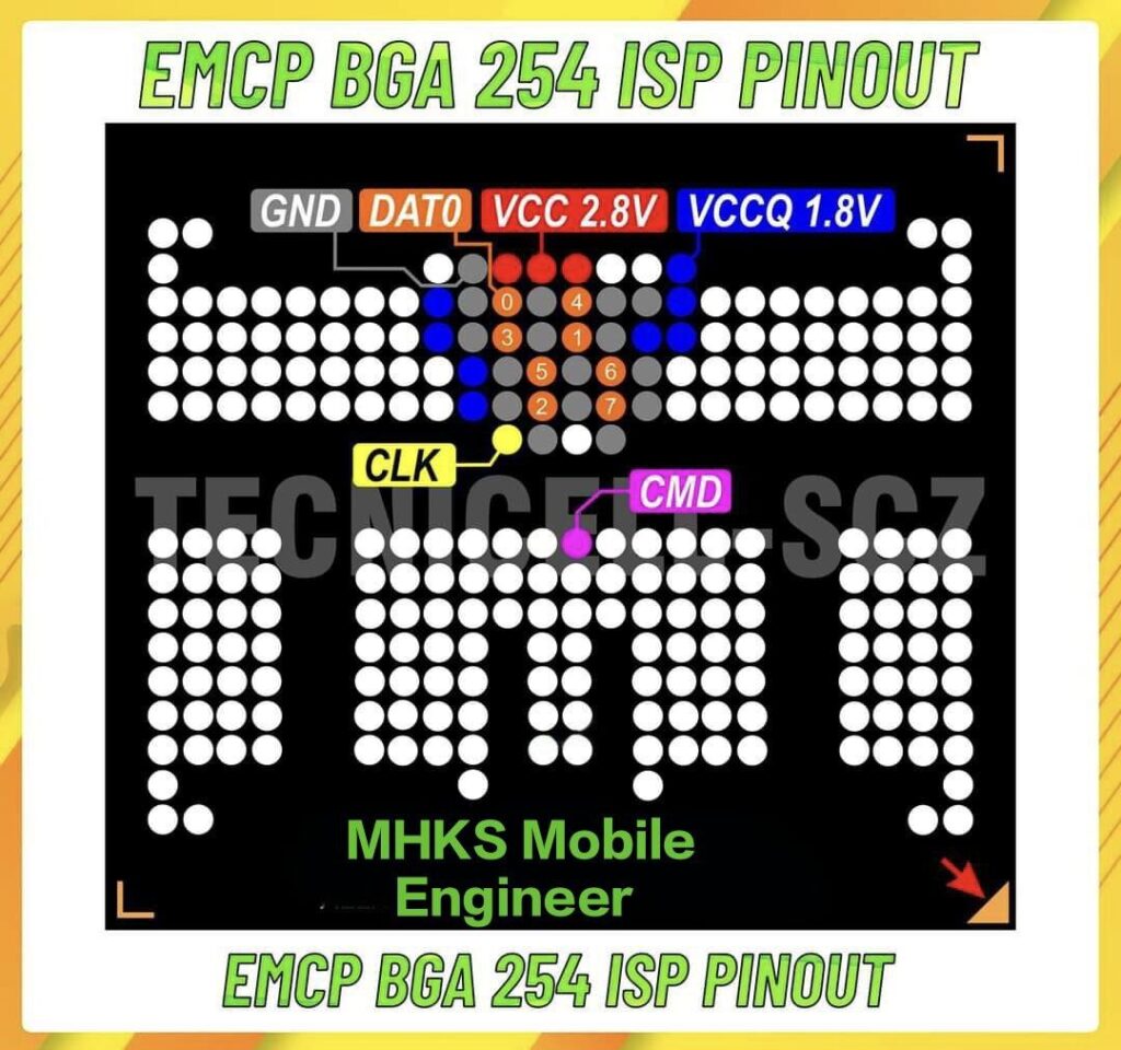
Here are the main signals you will commonly need when doing ISP on a BGA 254 eMCP / eMMC:
- CMD – command line.
- CLK – clock line.
- DATA0, DATA1, DATA2, DATA3 – data lines (in many cases only DATA0 is used for 1-bit mode)
- VCC (sometimes ~2.8 V) – the supply voltage for the eMMC core.
- VCCQ (sometimes ~1.8 V) – the supply voltage for the I/O interface.
- GND – ground reference.
- Possibly RESET_n or POWER_DOWN_n lines depending on device.
- Additional lines may be involved for 4-bit/8-bit bus width, RPMB, boot partitions etc.
Important Notes & Caveats
- The pin-out layout varies by manufacturer and by board: even though the package is BGA 254, different makers may map the balls differently.
- Many resources state you can get a “direct pin-out” for BGA 254 by using reference tools such as the UFI eMMC ToolBox.
- It is critical to use short jumper wires for ISP to avoid signal integrity problems. One forum post warns: > “Make jumper wire as short as possible.”
- Some boards have series resistors (especially on the CLK line) which may need to be bypassed, as noted by one technician: > “Take a look at CLK resistor, connect the jumper cable to the end of the resistor leading to eMMC.”
- Because of the variations and secrecy of many phone manufacturers, it’s difficult to guarantee a universal pin-out sheet for all BGA 254 eMCP chips. Many technicians rely on specialized adapters or tools.
Recommended Reference Diagram
Here is one clear diagram that many use as a reference for BGA 254 ISP pin-out:
You will see CMD/CLK labelled, VCC/VCCQ/GND, and Data lines marked accordingly.
Summary
If you’re attempting ISP on a BGA 254 eMCP/eMMC chip:
- Identify VCC and VCCQ volumes (commonly 2.8 V core, 1.8 V I/O).
- Identify ground.
- Locate CMD, CLK, DATA0 (or full DATA bus if applicable).
- Use very short wires.
- Confirm if any series resistor on the board needs bypassing.
- If possible, use a known adapter or tool that explicitly supports BGA 254 to avoid mis-wiring.
If you like, I can try to locate a full pin-ball map (ball grid layout with coordinates) for a specific manufacturer’s BGA 254 chip (for example Samsung, Micron, etc.). Would you like me to get that?