
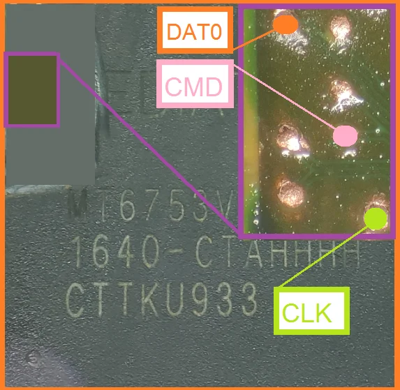
Key Pin / Signal Groups for UFS ISP Access
- Differential receive lane: RX0_P / RX0_N — for data from UFS to host.
- Differential transmit lane: TX0_P / TX0_N — for data from host to UFS.
- Reset / RST_N line for the UFS memory device.
- Low-speed control lines: e.g., M-PHY SCL / SDA, UniPro SCL / SDA — used for configuring and debugging the UFS link.
- Ground (GND) and power (VCC, VCCQ) supplies.
- Because UFS uses high-speed differential pairs, correct routing and pad access is crucial.
Why I couldn’t find a full diagram for MT6753V
- Many published pinouts are generic or for later MTK SoCs rather than MT6753V specifically.
- Some diagrams are behind technician-forums or paid service portals.
- The board-layout/test-points can vary significantly by device manufacturer (phone model), even though the SoC is MT6753V.
- Using an incomplete or incorrect pinout can damage the board (since high-speed differential signals are delicate) so publicly sharing is often restricted.
What you can do
- Identify the UFS memory package on your board (look for the UFS BGA chip near the SoC).
- Trace out test-points for RX0_N/P and TX0_N/P lanes — typically very near the UFS package or between SoC and memory.
- Look for very fine differential pairs labelled RX, TX lanes, or test-pads near the SoC.
- If you have access to a known Schematic for your exact board, that would give the ball/pad numbers.
- If you’re working with a repair-tool (e.g., ISP box) ensure you have the correct adapter and the correct version of the pinout for your phone variant.
If you like, I can try to search in service-manual / technician-forum archives (including non-English) for MT6753V UFS ISP pinout for a specific phone model (if you tell me the phone model) and see if I can locate a usable diagram. Would you like me to attempt that?