
Here’s the straight, honest situation regarding the MediaTek MT6735V ISP pinout for UFS:
❌ Official/Public ISP/UFS Pinout for MT6735V
As of now, there is no known official or verified ISP pinout schematic publicly available on technical repositories, datasheets, or indexed hardware-repair resources specifically for MediaTek MT6735V with UFS ISP connections. Searches for MT6735V ISP/UFS pinouts do not return any detailed pin arrangement, test points, or connectivity diagrams that you can reliably use for in-system programming (ISP) or direct UFS memory access. (Facebook)
Why There’s No Pinout Available
- The MT6735V is a relatively older/low-end MediaTek SoC whose documentation (including pin descriptions) is proprietary and not released publicly. Datasheets that do exist don’t include UFS ISP pinouts or test point maps. (datasheet4u.com)
- Most ISP/UFS pinouts shared online are for specific phone motherboards/devices, not for the SoC itself. They are often collected by repair technicians from board layouts rather than official documentation. (GSM Doctor)
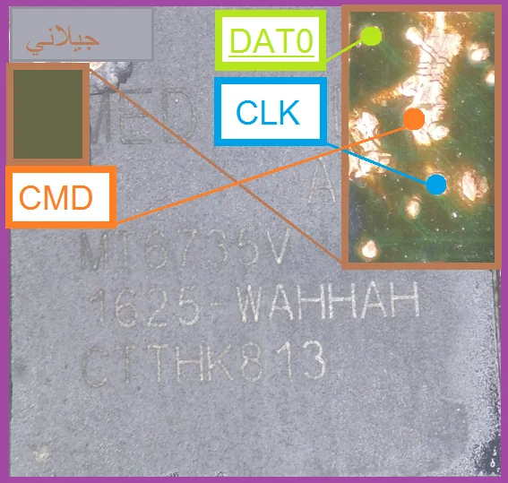
- Attempts to find MT6735V ISP/UFS pinouts sometimes lead to image galleries or forum snippets lacking usable schematic data. (emmc-ufs.com)
What ISP/UFS Pinout Typically Looks Like (Generic)
For UFS ISP access on most devices, the essential signals you’d need are:
- TX0P / TX0N – Transmit differential pair
- RX0P / RX0N – Receive differential pair
- CLK / REFCLK – Reference clock
- RST / RESET_N – UFS reset
- GND & power rails (VCC, VCCQ) – Ground and supply lines
These are the common differential and control signals for UFS memory interfaces used in ISP procedures, as seen in generic repair guides. (ZONA-EXPERTA2017)
Practical Notes for Hardware Repair Techs
- If you’re trying to dump or flash UFS memory on a device using MT6735V, the pinout will depend on the specific phone’s motherboard design, not solely on the SoC. ISP pinouts are often found near/between the SoC and the UFS chip on the board.
- Repair boxes (like UFI, Easy JTAG, Medusa Pro) rely on these test-points, but without a known schematic, you will likely need to visually trace board nets or consult a device-specific pinout resource.
- Some mobile repair communities/niche forums may have shared particular board pinout pictures for MT6735V devices, but these are not widely indexed or validated.
What You Can Try
- Search for device-specific pinouts for the phone model that uses MT6735V (instead of the SoC itself); these often include usable ISP/UFS test points.
- Use borescope/microscope + continuity probe to map UFS signal connections between SoC and UFS memory chip on the PCB.
- Refer to generic UFS ISP guides to understand signal roles (TX, RX, CLK, RESET, GND, VCC).
If you want help finding a device-specific MT6735V board pinout (ISP/UFS) for a particular phone model (e.g., Oppo/Realme/Xiaomi device using MT6735V), send the exact model and I can try to locate that for you.