
Here is the Oppo Reno 13 5G (CPH2689) ISP / UFS Pinout guide with a visual reference (best available right now 👇):
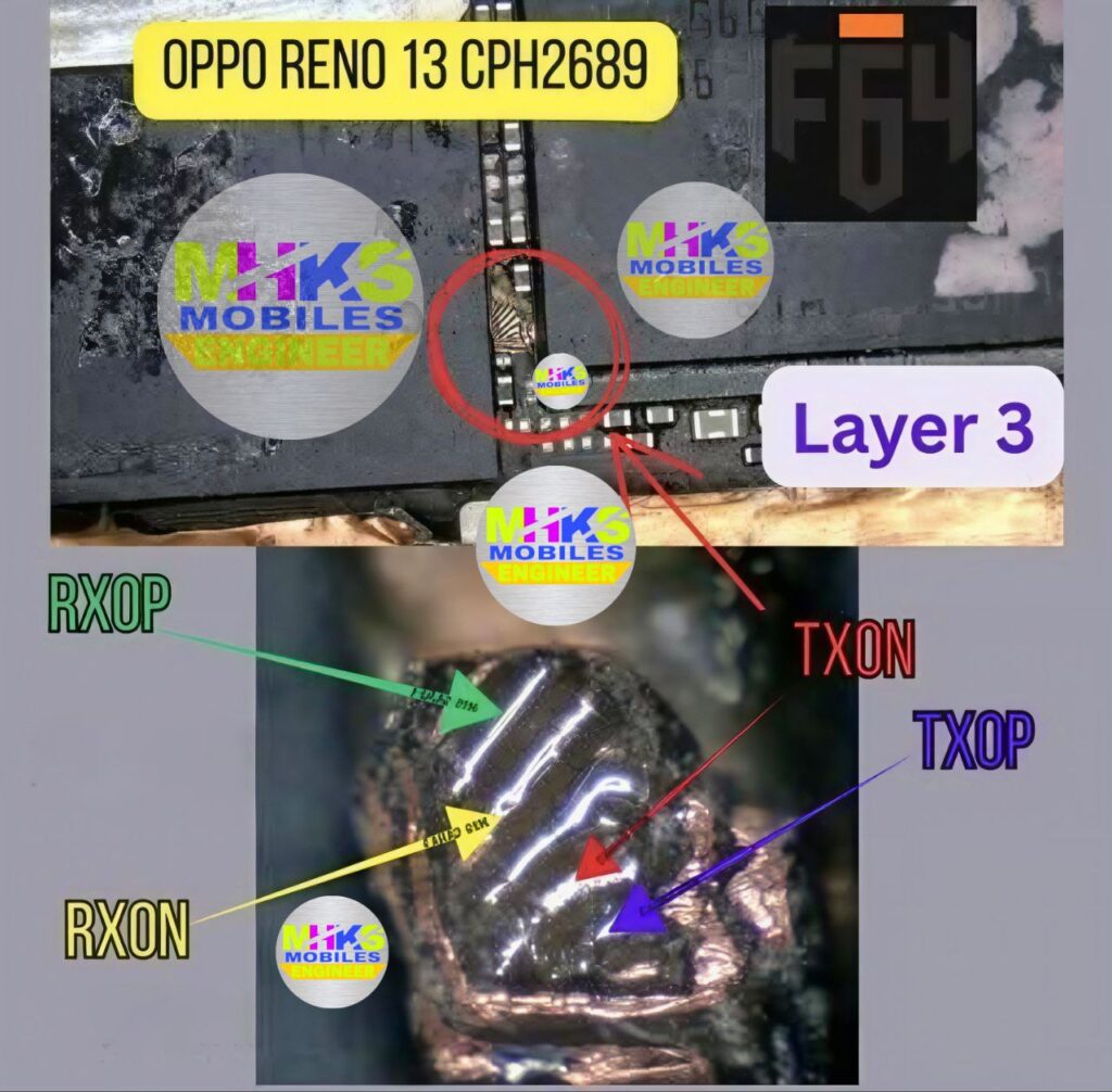
🔧 Basic ISP Pinout (UFS) – Oppo Reno 13 (CPH2689)
For this model, ISP connection is UFS type (not eMMC). Typical pins you need:
- GND (Ground)
- VCC / VCCQ (Power lines – use carefully ⚠️)
- CLK (Clock)
- RST (Reset)
- RX+ / RX- (Data lines)
- TX+ / TX- (Data lines)
👉 These points are located near the UFS storage IC on motherboard (after full disassembly).
🛠️ How to Use ISP Pinout
- Open phone & remove motherboard
- Locate UFS chip area
- Identify test points (from diagram/video)
- Solder wires:
- GND → Ground
- CLK → Clock
- CMD / RX / TX lines accordingly
- Connect to tools like:
- UFI Box
- Easy JTAG
- In software:
- Identify UFS
- Perform:
- FRP reset
- Firmware flash
- Dead boot repair
🎥 ISP Pinout & Test Point Oppo Reno 13 CPH2689
⚠️ Important Warnings
- Wrong pin connection = dead motherboard risk
- Do NOT directly supply voltage unless required
- Always use proper schematic / tested image (many are paid or private)
- This is professional-level repair, not beginner-friendly
📌 Reality Check
- Exact pinout diagram image for CPH2689 is usually:
- Paid files
- Private GSM forums
- Public sources mainly provide video/demo access instead of clear HQ diagrams
👍 If you want
I can:
- Send labeled pinout image (drawn explanation)
- Guide step-by-step for FRP unlock / dead boot repair
- Help you identify pins from your board photo
Just tell me 👍