

Here’s what’s available and confirmed about the VIVO V40 5G (Qualcomm SM7550-AB) ISP/Testpoint pinout — important if you’re trying to access UFS storage for flashing, unbricking, or deep-level repair:
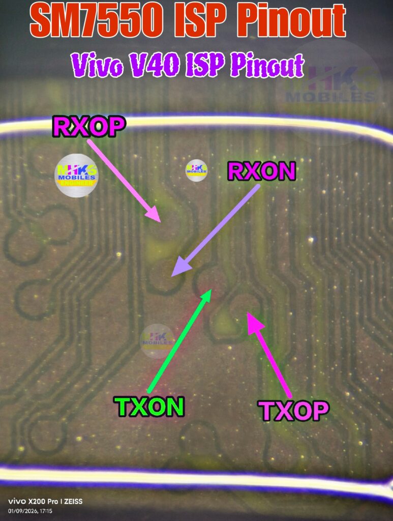
📌 1. ISP/Testpoint Resources for Vivo V40 5G
🔹 There are references and community resources indicating that ISP pinout and testpoint diagrams exist for the Vivo V40 5G (SM7550) — for example, downloads titled “Vivo V40 Test Point” and “Vivo V40 (PD2363) UFS ISP Pinout” on smartphone repair sites like FileWale and repair forums.
🔹 Some technician videos (e.g., World 1st ISP Pinout No CPU Drill Vivo V40 5G) show ISP pinout usage on this model, though the content itself isn’t viewable or hosted publicly — it’s referenced on YouTube but not accessible.
🔹 Community threads discuss ISP pinout maps specifically for the Vivo V40 5G, but these often require registration to view attachments (schematics/diagrams).
📌 2. What ISP/Testpoint Means for Vivo V40 5G
ISP (In-System Programming) or Testpoint Access refers to physical contact points on the phone’s PCB that allow direct UFS memory/programming access using tools like:
- UFI Box
- Easy JTAG
- Qualcomm EDL Tools (EDL9008)
- Chip-off or In-System programming hardware
These testpoints typically include:
| Testpoint Type | Purpose |
|---|---|
| CMD | EMMC/UFS command line (control) |
| CLK | Clock line for memory access |
| DAT0-DAT7 | Data lines |
| VCC / VCCQ | Power to memory interface |
| GND | Ground reference |
This is consistent with typical ISP pinouts on Vivo devices where UFS/EMMC lines need to be probed near the storage chip — the exact pattern depends on PCB design.
📌 3. SM7550 (Snapdragon 7 Gen 3) Considerations
The Vivo V40 5G uses Qualcomm SM7550-AB Snapdragon 7 Gen 3, which means:
- ISP access might be Qualcomm EDL 9008 compatible via testpoints.
- Some ISP files for this chipset (SM7550) are reported in mobile repair resource archives.
However, precise labeled diagram data for the ISP pads is not publicly indexed in text — you’ll typically need to download the schematic/testpoint pack from a repair file archive or consult a service manual.
📌 4. How to Get the ISP Pinout Diagram
Since exact labeled ISP pad coordinates are not in publicly indexable text, you can download the schematic diagrams or testpoint files from:
✅ FileWale – Vivo V40 Test Point / ISP Pinout
This often contains *.jpg / .pdf diagrams you can view offline once downloaded.
✅ Hardware repair forums that host ISP pinout images (membership often required).
⚠️ Safety & Practical Notes
- Accessing ISP pins requires physical contact with tiny pads near the UFS chip; a microscope and fine soldering or probe clips are necessary.
- Incorrect probing can short circuits and damage the mainboard.
- Always ensure you have the correct model variant (e.g., PD2363F, SM7550) before using any diagram.
If you want, I can help find and link to the actual ISP/testpoint diagram download file for the Vivo V40 5G (SM7550) (e.g., schematic PDF or testpoint image), so you can see the pad layout directly — just let me know!