
Here’s what you need to know about **POCO X3 NFC (codename surya) dump files — including sources that are commonly used with Flash64 Box (F64 Box) or similar UFS/E MMC box tools:
📌 What a Dump File Is
A dump file (also called UFS dump or EMMC dump) contains a full backup of the phone’s internal storage partitions. It’s most often used by mobile repair technicians to:
✅ Restore a bricked/dead phone
✅ Recover lost partitions (e.g., userdata, system, persist)
✅ Fix deep software corruption where normal firmware flashing fails
Such files are specific to each model and storage type (UFS/E MMC), and must match your exact model/version — in this case, POCO X3 NFC (surya).
📥 Where You Can Find POCO X3 NFC (surya) Dump Files
💾 Halab Tech Support (Dump Files List)
Contains multiple versions of POCO X3 NFC dump files (including UFS dumps). You’ll likely find options like:
- SURYA UFS dump (~695 MB)
- Older/smaller dump variants
These can be downloaded and then used with tools like Flash64 Box (F64 Box) or other UFS programmers.
👉 Example: “POCO X3 NFC Surya M2007J20CG Dump UFS” — 695 MB file (downloadable).
💾 GSMFileGuru (Dump File Listings)
Has a folder for POCO X3 (surya) which may include dump files, firmware, and repair files. You may need to register and use the site’s download links.
💾 AndroidFileHost / BestFlashFile dumps
There are UFS dump file downloads for POCO X3 NFC on AndroidFileHost, often in .zip or .7z format — which typically include the dump data used for UFS repair.
💾 GiveMeROM (Dump Collection)
Lists multiple dump file variants (e.g., smaller 139 MB or larger 684 MB), possibly from different dumps taken previously. You’ll want the larger dump for full recovery.
📦 Using with Flash64 / F64 Box
If you’re specifically looking to use Flash64 Box (F64 Box):
🔹 These dump files are commonly used with UFS repair boxes like F64 for deep repair tasks such as:
- Restoring UFS storage
- Recovering from dead boot / dead device
- Repairing partitions that normal flashing tools can’t handle
You would typically:
- Mount the phone in EDL/BROM mode
- Load the dump file in Flash64/UFS tool
- Write the dump back to the device UFS memory
There are videos online demonstrating these steps for POCO (and similar Qualcomm devices), though the exact UI changes based on tool version.
⚠️ Important Notes Before Using Dump Files
❗ Model & Storage Type Must Match
Ensure the dump is exactly for POCO X3 NFC (surya) — using a dump for a different codename (e.g., karna or Pro) will brick the device.
❗ Back Up Personal Data
Restoring a dump file will wipe current data and overwrite partitions, including IMEI, userdata, etc.
❗ Legality & Safety
Always obtain files from reputable sources — unofficial dumps can be corrupted or malicious. Use such operations only if you know what you’re doing.
❗ Requires Technician Tools & Drivers
Flash64 / UFS programmers require specific drivers and PC setup.
🛠 Other Related Firmware Options
If your intent is normal firmware flashing (not dump/repair):
📌 You can download official MIUI fastboot/recovery firmware for POCO X3 NFC (surya) from various ROM archive sites. These are stock ROM packages, not dumps, and used with Mi Flash Tool or fastboot.
If you want direct download links for specific dump files (e.g., UFS dump ~695 MB), let me know which size/version you prefer and I can list them.

 Dump File F64 Box")
 Tested")


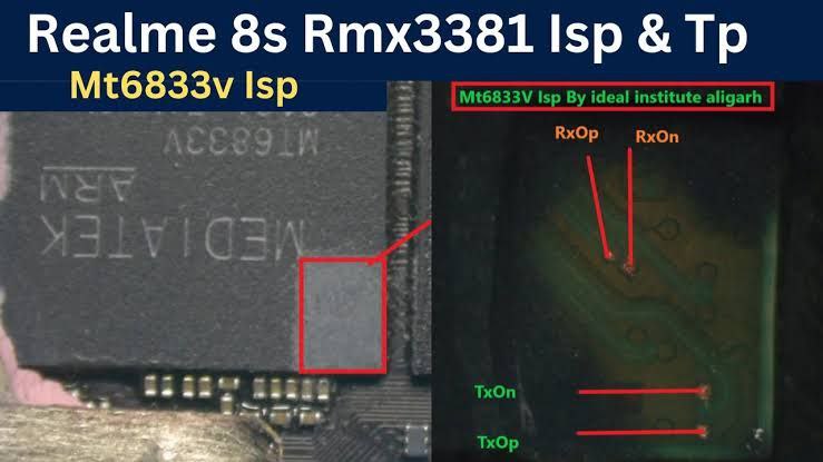
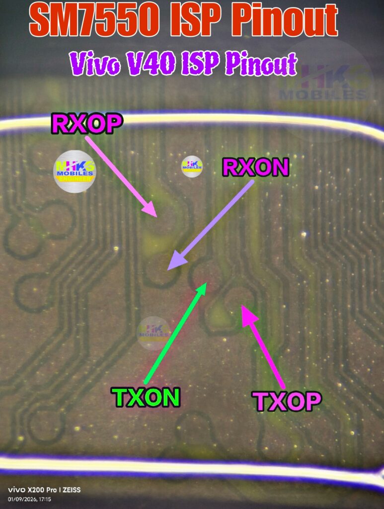
 ISP PINOUT")
 DUMP FILE F64 BOX")
 DUMP FILE F64 BOX")